 Аудио-википедия
База знаний по hi-fi и high-end технике и комплектующим, отзывы и впечатления
Инструменты пользователя
Боковая панель
DN2540 High Voltage Constant Current Source
https://www.monoandstereo.com/2013/11/dn2540-high-voltage-constant-current.html?m=1
DN2540 High Voltage Constant Current Source
Ever dreamed of getting the highest possible linearity out of your triode gain stage, by means of using an extremely high value of an anode resistor, say 1 Meg or more? If only that would be possible, we would have a nice, almost flat, load impedance line on our anode characteristics, and the resulting high linearity response and transfer characteristic of our triode gain stage that goes with it. And this would be valid for almost any triode that you could possibly use or imagine. What a pity that we cannot use such a resistor. Why? Each and every tube needs to have some current flowing through it, be it for the sake of positioning oneself on an operating point of the tubes anode characteristics that provides reasonable working conditions.
Let’s assume that a reasonable current flowing through our tube of choice is 10mA and that such a current puts us in a nice area of it’s characteristic. So we need this current to flow through the tube, so as to “define” the DC working conditions of the tube. But now, look what happens: If you were to “use” that 1 Meg resistor, this would imply that:
a). The resistor would need to drop a voltage in the order of:
0.01A * 1 000 000 R = 10 000 Volts.
This would be no ordinary power supply, to say the least.
b). The power rating of the resistor would need to be substantial:
P = I * I * R = 0.01A * 0.01A * 1 000 000 = 100 Watts.
Not feasible.
But not all is lost. Signal-wise, what we are really interested in, is not a “DC impedance” as seen from the anode, but rather the “AC impedance”, because we shall be amplifying AC signals, and it is this AC signal that we would like to have “exposed” to such big impedances, as seen from the anode.
There is a “method” do get the best of both worlds. A healthy DC current flowing through the tube, the current that is used to “define” the operating conditions of the triode, and obtained from a reasonable power supply voltage, of say up to 200 ~ 350 Volts. But at the same time, from the point of view of AC signals, an “AC” impedance in the order of 1 Meg or more.
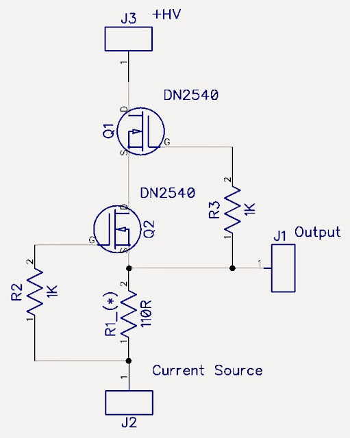
Have a look at this following circuit, and let us analyze what is happening here …

What we have here is a “contraption” that I intend to put “on top” of the anode of my triode.
It is powered by some reasonable value of high voltage, high enough to obtain the necessary DC operating conditions for the elements as depicted and the triode underneath, high enough so as to achieve the required AC output signal swing, but on the other hand, low enough so as to not to stress the components too much.
The transistors that are used are so called N-MOS depletion mode transistors. These are a very special kind of silicon device. They are basically “silicon triodes”. A minor difference is that they do not need an extra filament / heater supply.
If you do NOT provide these devices with any voltage on their gates, they will be normally conducting. Open. Just like a vacuum tube, a triode, that does not have any control grid potential. Such behavior opposes “traditional” (i.e. enhancement mode) Mosfet’s, where you actually need to apply some voltage to the gate to “open them up”. But here, these depletion mode Mosfets, they actually behave sort of like a silicon “tube”. They normally conduct. In order to “close” them, you need to apply a negative voltage to the gate. Now, look at the R1 resistor { (*) the value of which needs to be fine tuned on a case by case basis }. It is very similar to a Cathode Resistor in a tube circuit, and it creates “negative bias”, which is passed over, via R2, to the gate of the Q2 “silicon tube”. A very normal case of “auto-bias”, if viewed as a ‘tube analogy’.
Now, let us assume that we need a 20 mA current flowing to the tube underneath, and let us assume that the Q2 device conducts such a current in the case of a negative gate voltage of 2,2 Volts. This would imply that we need a “current programming” resistor R1 with a value of 2,2 V / 20 mA = 110 R. Alternatively, if we would wish to reduce this current by half, so as to obtain, say, 10mA of current flowing down to the tube, we would use a different value of such a current programming resistor, mainly: 2,2 V / 10 mA = 220 R. You get the idea.
Now, what happens if the tube tries to “pull” a higher current ? As soon as any minuscule increase of current takes place, this will translate to an increase of the voltage drop on the R1 programming resistor, so the “negative bias” voltage herewith would increase and be passed on to the gate of the Q2 device (= “silicon triode”). A more negative gate (“grid”) voltage implies a reduction of conduction, so the Q2 device will obviously “oppose” to any increase of current. And vice verse: if the current were to decrease in value, this would imply a slightly diminished negative bias, and hence the Q2 device would “open up” a little more, so as to compensate.
But to what extent will it “oppose” any current changes? Easy. The Q2 device will use all of it’s trans-conductance, which, as per documentation available for this chip, may be in the order of 325 mA/V. All of this transconductance will be used to maintain the status quo.
To put this into perspective, an intuitive example: if our “programmed current” of 10 mA should change (increase) by say 1 micro Ampere (just a mental assumption), that would imply a change (increase) of the negative bias voltage of 220 R * 1 micro Ampere = 220 micro Volts = 0,22 mV = 0,00022 V. Multiply this change by 325 mA / V of transconductance, and you can clearly see that such a small voltage change on the gate would (assuming all other conditions being constant) imply a 71.5 micro Ampere change (decrease) in the current flowing through the device. Obviously, that is but only the “potential capability”. The current will not fall by such an amount, as the initial “deviation” of the current, the one we started off with, was only but 1 micro Ampere. Any decrease in current corresponds to a decrease of the negative auto-bias. But what I am trying to visualize here is the “self-regulating” feature of this setup: the Q2 device shall use it’s full force, all of it’s available trans-conductance, solely for the purpose of “opposing” any change.
But what about Q1 ? The upper DN2540? Why do we need that one? Look at it this way: from the Q1′s point of view, it’s “cathode” is similarly loaded with an “auto-bias” resistor. But one that is “variable” in value. This “variable resistor” is comprised of the Q2 device.
Earlier, we said that the the current flowing through these serially connected devices is 10 mA. Therefore, the voltage on top of the Q2 device takes on such a value, so that the gate of Q1 is also set with a negative bias voltage of about ~2,2V, i.e. enabling it to conduct exactly the “programmed” 10 mA of current that is needed.
Now, please recall that scenario, where the lower Q2 device needed to “compensate” for a (fictitious) increase in current flow. We said, that it would have be biased more negatively, and hence Q2 would decrease it’s current flow. But Q1 would see this as an “increase” of the value of it’s “cathode” auto-bias resistor, because Q2 is the “variable resistor” sitting at the cathode of Q1. Such an “increase” of the cathode resistor also results in a higher value of the negative bias voltage on the gate of Q1, so Q1 will actively participate in decreasing the flow of current. The upper device, Q1, would “assist” Q2, to the full force of the transconductance that it has available, in the process of “decreasing”, or “correcting” the current, that “became too high”.
What we basically have here is a cascaded circuit. A single device would use all of it’s transconductance, i.e. the 325 mA/V to oppose the current changes. But within a cascade, we have effectively achieved a “super-device” that can achieve a breathtaking “super-transconductance” of 325 * 325 = 105625 mA/V … Well, sort of simplified, but you get the idea.
But how does this all “affect” our triode underneath ?

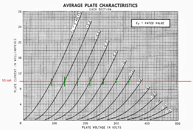
Basically, our triode “sees” nothing more than a CONSTANT 10mA. The triode as above, a popular 6SN7, for example's sake, it does not know the “how” and the “why”. And frankly speaking – it does not care. This current will be very stable, irrespective of what the tube tries to “do” with it. From the perspective of your tube’s anode characteristics, you shall be basically stepping along a horizontal load line. It will be a horizontal line, and it will be (obviously) the 10 mA line. Nice. Any change in the gate voltage upon the triode will translate into voltage changes on the triode. If the triode’s cathode is ground referenced, exactly the same voltage changes will be observed on the anode, and on the output of the CCS. The output of this gain stage (specifically: the upper end of the R1 current programming resistor) will closely follow the anode voltage. The difference will be a constant offset of 2,2 V – it is the auto-bias voltage difference. As we by now know, this value is constant, hence the output voltage, in AC terms, is an exact replica of the AC signal on the anode of our triode. It is only but DC shifted by 2,2V higher.
Please also note the linearity. Do you see it? If not - a small hint: Look at the amount of square boxes between the green marker lines. The amount of boxes spanning between the marker lines crossing the «0V» and «-2V» grid voltage curves is nearly exactly the same (~8 boxes) as the amount of boxes spanning between the marker lines crossing the «-2V» and «-4V» grid voltage curves …. The same goes on with the «-4» to «-6» and so on. Small variations exist, but generally, this is looking very good.
But there is more.

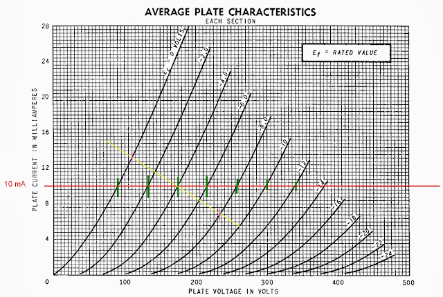
Consider a grid voltage with an 8 volt P-P input signal, swinging from 0V to -8V around the mid point at -4V. The CCS load would give an output voltage spanning from 90V do 257V, or a 167 V P-P. Such an output voltage swing could be possible to obtain from a power supply of (guessing) 280V, leaving a healthy 23 V of voltage overhead for the Q1 and Q2 devices.
A resistive load, of say 20k, on the other hand, resembled as a yellow diagonal line sloping downwards to the right, would yield a much smaller amount of output voltage swing, spanning from 110V do 232V, or a 122 V P-P. This is a significantly lower voltage swing that the 167V p-p, possible to obtain from a reasonable power supply voltage.
But please also note another potential pitfall: 10mA across 20K is an additional voltage drop of V = I * R = 200 V across the resistor alone, so the power supply voltage would need to be something like 370 V (the whereabouts of where the yellow line would cross the «zero» mA axis), and such a voltage is a hazard in itself, because the tube might simply not withstand such a high voltage and arc over.
Returning to the CCS, the value of R1 needs some tweaking, as the individual characteristics of each and every DN2540 will vary slightly. Each and every unit may require a slightly higher or lower bias voltage to obtain the required 10mA. Hence, variations in the exact value of R1 are unavoidable.
Such a CCS is also a very good means of increasing ripple rejection, ripple originating from a less-than-perfect filtering with the power supply. As mentioned earlier, th CCS is basically a high impedance. Imagine a voltage divider, consisting of a 1 Meg resistor at the top, and the tube’s internal Ra at the bottom. The ratio of such two resistors, the high impedance of the CCS compared to the much smaller plate resistance of the triode defines the ripple rejection ratio, or the PSRR («Power Supply Rejection Ratio»). So even if there is a significant amount of ripple at the “top” of the 1 Meg impedance, there is close to nothing left of it on the comparatively low plate resistance of the triode.
Another good feature of the CCS setup, based on Q1 and Q2 depletion mode Mosfets, is a low internal reactance. This implies that the CCS will maintain it’s “high impedance” across a broad range of frequencies, meaning that the CCS is a broadband type of device.
The attentive reader might have noticed a mu-follower type of quality in the way in which we take the output signal from this circuit. Indeed, the output signal is rather taken from the source of the lower Mosfet, and not directly from the anode of the triode. If you are concerned about the high capacitance and / or load introduced by the following stage, this CCS setup, sitting on top of your triode, is also a very good overall performer. The triode is isolated from the load capacitance by the current programming resistor. The following stage, with it’s low impedance and possibly high reactance, is now driven from low impedance of the source pin of the Mosfet. There is no direct connection between anode and load. The triode is hence «isolated» from the load.
Happy soldering. And while you are at it, please do not forget to calculate the potential heat dissipation on these Mosfets – especially on the one on top, which will “take on” the bulk of the high voltage. It is very probable that this upper Mosfet shall need a healthy radiator, and that it will run hot. To put this into perspective: If it is conducting 10mA and dropping say 100V – this essentially means a heat dissipation of 1 Watt. But there will be times, where the voltage spanning this transistor will be close to the full power supply voltage. So check your figures and see if you need the radiator.
Regards,
http://hiend-audio.com
zjj_wwa@hiend-audio.com
