 Аудио-википедия
База знаний по hi-fi и high-end технике и комплектующим, отзывы и впечатления
Инструменты пользователя
Боковая панель
Содержание
CCS
Active loads and signal current control
The use of active loads (CCS’s) in vacuum tube amplifiers has several advantages over resistive loads. These including full mu of the tube, lower distortion, and greatly improved power supply noise rejection.
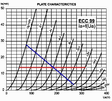
When using active loads the load line presented to the triode is a horizontal line versus the diagonal line seen by resistive loaded stages. Transformer and choke loading also provides a horizontal load line in the midrange frequencies but goes reactive at low frequencies where the inductance limits the performance and at high frequencies where the inter-winding capacitance limits the performance.
The horizontal line represents the load line when using a CCS plate load. The diagonal load line represents a 15K resistive plate load. Working off the too small graph we can determine roughly that with a 12 volt P-P input signal the resistive load would give an output voltage of 188 volts P-P where the CCS load would give an output voltage of 269 volts P-P. If you compare the spacing of the grid curves you can see that with the CCS load the lines are much more evenly spaced.
Active loads are also very good at increasing power supply isolation. The CCS appears as a very high impedance low reactance load. The ratio of the high impedance of the CCS against the plate resistance of the triode determines the power supply isolation (ripple rejection). I prefer the use of the term power supply isolation instead of ripple rejection as it offers a more comprehensive view of workings of the amplifier. The low reactance means the CCS will remain a high impedance load over a very wide range of frequencies.
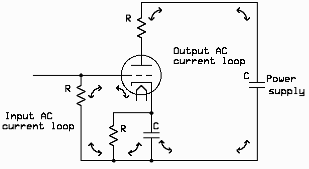
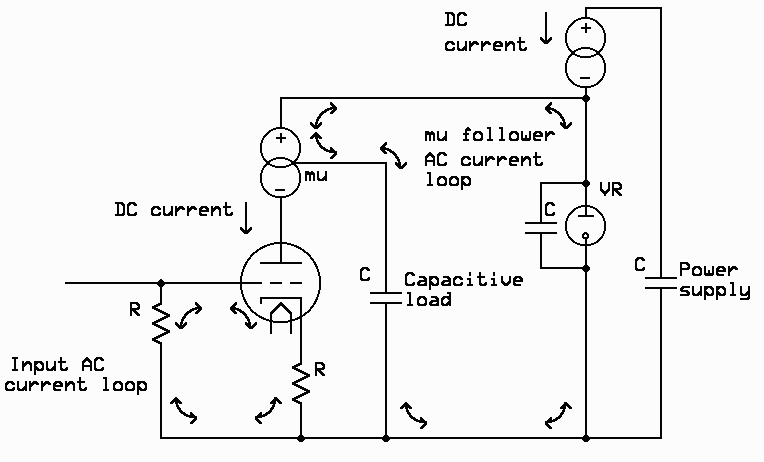
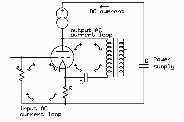
Active loads are also a tool that can be used to control where the AC signal current flows. When active loads are coupled with shunt regulators, the use of large capacitors in the signal current loop can be avoided.
One of my design goals is to have the power supply responsible only for supplying DC current for the operation of the stages and to have the AC current paths separate from the power supply.
Conventional SE stage
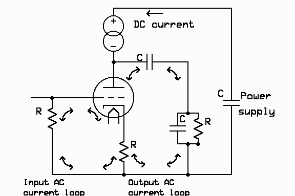
In conventional SE circuits the power supply is an integral part of the signal current loop. This makes for a signal loop that has at minimum, 4 components in the AC path, the plate load, power supply capacitor, cathode bypass capacitor and the triode. In most cases, the cathode bypass cap and the final capacitor in the power supply are large capacitors, usually electrolytics that have less than stellar sonics. Another problem that plagues conventional SE circuits is poor power supply isolation.
SE stage with active load
When we add an active load the basic operation of the stage changes. Now the power supply only provides DC operating current as the CCS provides isolation between the power supply and the triode. With the CCS holding the current drawn from the power supply steady the demands on the power supply are greatly reduced.
The great power supply isolation provided by the CCS makes the design of the power supply much less critical. Depending on the performance of the CCS, power supply isolation of over 100dB is possible. It is not necessary to have super low ripple and noise with this kind of isolation available.
Another feature of having the current through the triode held constant by the CCS, we can dispense with the cathode bypass capacitor. The constant current flowing through the cathode resistor provides a constant DC voltage to bias the stage. Effectivly the stage operates with fixed bias.
This holds for light loads driven by the stage. If the next stage is a heavy load requiring current to be delivered the tube will come out of constant current operation. In RC and DC coupled circuits the predominant load is usually the miller capacitance of the next stage. The capacitive load causes the horizontal load line to become elliptical at high frequencies increasing the distortion. This could be one of the contributors to harsh, strident, grainy high frequency sound.
To overcome the loading issues a follower circuit can be used to isolate the load from the triode. The CCS’s I have designed have the capability of performing as a source follower without any modifications. This could be viewed as an advantage to having the voltage reference and current setting hardware at the bottom of the CCS.
Before moving on to the follower ideas, a basic understanding of CCS operation is necessary.
Overview of a simple CCS
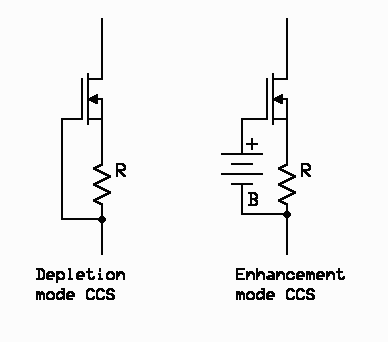
One of the simplest CCS’s to setup uses a single mosfet. There are 2 kinds of mosfets that can be used to build CCS’s. Depletion mode mosfets are normally «on» and enhancement mode mosfets are normally «off». It only takes a single resistor to make a CCS with a depletion mode part where it takes a voltage source (battery) and a resistor to build a CCS from an enhancement mode mosfet.
To use a depletion mode mosfet as a CCS the fist step is to refer to the part’s data sheet. Find the performance curves plotting current Vs drain voltage. They will look like nice pentode plate curves. Look for the bias voltage at the current you want the CCS to operate at. The value of the current set resistor will be the bias voltage divided by the operating current. The value may need to be adjusted slightly to get due to turn-on voltage variations in the mosfets.
To use an enhancement mode mosfet as a CCS we need to provide a bias voltage (battery) to turn the mosfet on. You will need to refer to the data sheets to find what the turn-on voltage is at the required current. The value of the current set resistor will be the battery voltage minus the turn-on voltage of the mosfet.
The disadvantage to single mosfet depletion mode CCS’s is relatively poor performance. When using the depletion mode mosfet as a CCS the bias voltage available to set the current is usually 1 volt or less. The low bias voltage does not provide good feedback to stabilize the operating current.
When using enhancement mode mosfets with batteries to provide bias the voltage can be up to the gate voltage limit of the mosfet, typically 20 volts. The higher voltage provided by the batteries provides much better internal feedback in the CCS. This increases the performance by a large margin. Batteries can also be used with depletion mode mosfets to improve the performance of the CCS.
Another poor performance aspect of single mosfet CCS’s is high shunt capacitance. Mosfets look like great parts until you take into account their high capacitance issues. I suspect that the shunt capacitance is the source of most of the sound coloration’s that make CCS’s sound different.
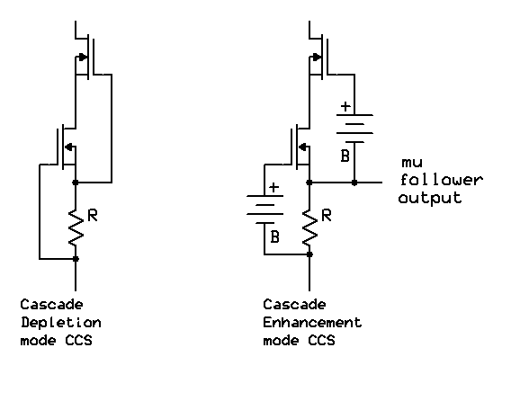
The use of a cascade circuit configuration will greatly reduce the shunt capacitance and improve the DC performance of a CCS.
Performance in a cascode circuit improves because the upper mosfet isolates the lower mosfet from voltage variations. At higher frequencies where the capacitance issues come into play the AC leakage current that couples across the drain to the gate of the upper mosfet is routed back into the current summing node of the CCS, the source of the lower mosfet. There will be very little AC leakage current from the drain to gate of the lower mosfet, as it is isolated from the AC signal by the upper mosfet. With the upper mosfet handling the AC signal voltage the lower mosfet basically operates at DC.
Using a CCS as a combined CCS and mu follower
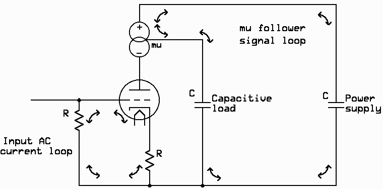
When an n-channel mosfet is used for a CCS we have an opportunity to get a second function almost for «free». The output signal can be taken from the source of the lower mosfet instead of the plate of the triode. Refer to the schematic above to see the circuit detail of where the signal is taken from.
When driving output triodes or interconnect cables that are high capacitance loads, this arrangement works very well. The driving triode is isolated from the load capacitance to maintain constant current operation at high frequencies and the next stage is driven from low source impedance.
The drawback to this arrangement is the current to drive the next stage comes from the power supply, it violates the design concept of separate paths for AC and DC.
CCS fed shunt regulators
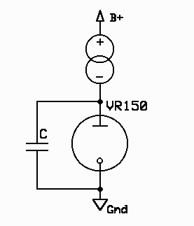
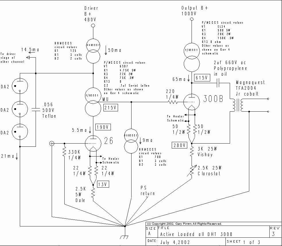
A CCS feeding a VR tube forms a simple shunt regulator circuit that has excellent performance (and the glowing VR tubes look great too).
Shunt regulators work by varying the current they draw from a circuit to maintain a fixed voltage. If the voltage tries to increase the shunt regulator increases the current it draws. Conversely, if the voltage starts to decrease the shunt regulator decreases the current draw to hold the voltage stable. The simplest shunt regulator is the VR tube or «gas zener».
Depending on VR tube family the operating current can be from 3ma to 40ma. The miniature tubes generally are 3 to 30 ma while the octal tubes are 5 to 40 ma.
VR tubes are quite inductive. To improve the high frequency performance a small capacitor can be added in parallel with the VR tube. Most VR tubes have a maximum capacitance specification of .1uf. If the capacitance is increased above .1uf the VR tube and capacitor can form a relaxation oscillator and will start to oscillate. I have been using .056uf capacitors with good results.
A CCS fed shunt regulator is placed between the power supply and the CCS feeding the triode. This isolates the signal path from the power supply.
To setup a CCS fed shunt regulator in this application you set the upper CCS for the current that the lower CCS is set for plus the current to bias the VR tube. Assuming the lower CCS is set to deliver 10ma to the triode and the current desired in the VR tube is 15ma, the upper CCS would be set to deliver 25ma.
It is interesting to note that only the circuits using the mu output have the triode operating in true constant current mode. In the other variations of CCS loaded triodes where the signal is taken from the plate, the plate current varies in proportion with the load current.
CCS loading of output stages
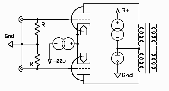
Output stages are a different case. The CCS is used as a high performance replacement for the plate choke. The CCS offers performance that is simply not achievable with inductors.
The object is not to operate the triode at constant current but to provide the output stage with a constant bias current that does not change over the operating frequency range of the amplifier.
In this arrangement the output stage as a whole operates at constant current. With the triode working into the load presented by the output transformer. The sum of the AC currents through the triode and the primary of the output transformer will equal the DC current set by the CCS.
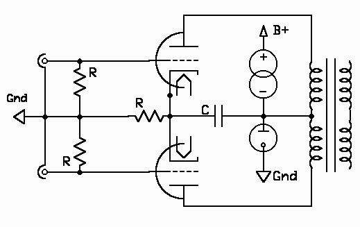
The use of CCS’s use in P-P stages
There are a couple of ways that CCS’s can be used in P-P stages.
CCS fed shunt regulator to feed the plates. This provides a stable clean supply for the stage.
A CCS can be used on the cathodes of a P-P input stage. This allows the input stage to perform the phase splitting duties.
Copyright Ó Gary Pimm 2003. All rights reserved
Варианты применения
April 14, 2008
Due to continued interest in building the self bias CCS and my lack of time to sell boards I've decided to release this version of board layout to the public domain. If you have batches of boards made up for whatever use drop me an email. I'd like to hear about what you use them for. You will find a zipped board file in the down loads section.
To use the board file you need to install the latest version of ExpressPCB then open the file. Ordering 1 mini board set using this file gets you 12 self bias CCS boards. You will need to use a large pair of shears to cut the boards apart.
You are responsible for determining the suitability of the CCS circuits for your intended purpose. The author is not responsible for personal injury or property damage caused by use of the information on these pages.
Updated 3/20/05
Here is the newest member of the CCS family. It was created by using the layout of the new battery biased CCS and replacing the batteries with the voltage reference from the Rev. 5 CCS.
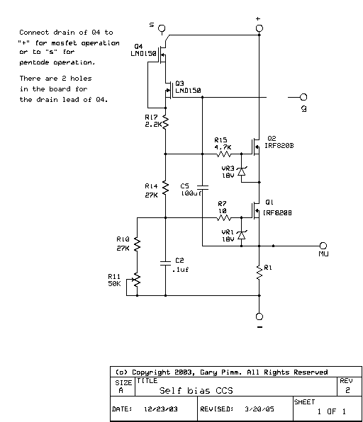
With the new voltage reference the self bias CCS starts softly. Initially, the current is only that of the reference, .35ma. As the voltage reference charges up C5 the CCS starts to conduct. It takes ~20 seconds to reach full output.
For choosing the value of R1 the voltage range of the reference is 9.5 to 27 volts. The turn on voltage of the MOSFETs is approximately 3.5 to 4 volts so the voltage range seen by R1 will be in the 5.5 to 23 volt range. Allowing for the variations in SS parts a working range of 8 to 20 volts should be available. The design center for R1 is 14 volts.
If you want to minimize the voltage requirements of the CCS R1 should be chosen to deliver the desired current at the low end of the adjustment range. R14 can be reduced from 27K to 15K to lower the minimum voltage required by the CCS by 4.2 volts.
The tradeoffs of these changes are minor but present. Lowering the value of R1 reduces the local voltage feedback reducing the effectiveness of the CCS slightly. In circuits where the CCS is use as a plate load for triodes reducing the value of R1 increases the noise gain can increase the noise floor in low level circuits. The noise gain is basically the plate resistance of the triode divided by the value of R1. Reducing the value of R14 could increase the shunt capacitance by a small amount as Q1 will have less voltage across it. Decreasing the voltage across MOSFETs below 10 volts quickly increases the capacitance.
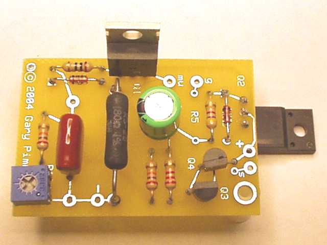
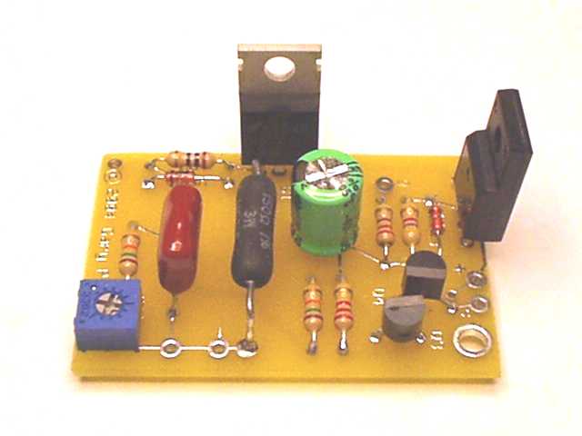
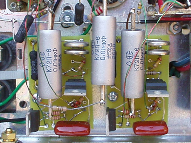
Here is a self bias board setup for MOSFET only operation with Q2 on the back of the board to allow using the top plate as the heatsink. When operating the CCS's over ~90ma Q1 needs to have a heatsink also, either a small clip-on heatsink or Q1 can be mounted on the back side just like Q2 is shown here.
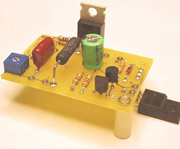
Another angle to help show how Q2 gets attached to the chassis
The standard TO220 package has enough lead length to allow for the use of either 10mm or 1/2 inch standoffs, depending on what standard is used in your country.
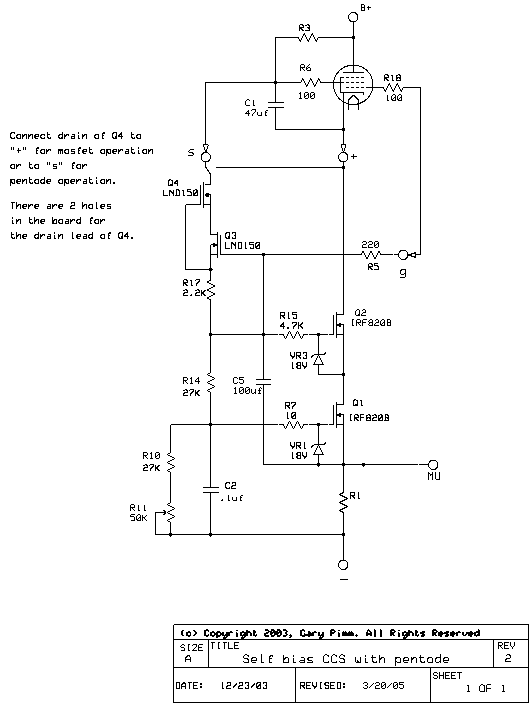
Here is the schematic of the self bias CCS.
The self bias board supports the option of using a Pentode for higher voltage/power/performance applications. This is basically the same circuit as the Rev. 5 with the Pentode support parts mounted off the board.
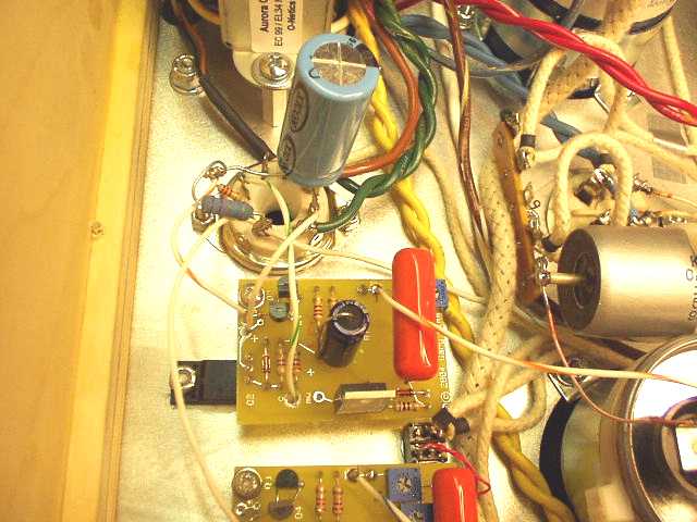
Here's an image of a self bias board setup for operation with a Pentode in an Amity amplifier feeding the VR tube on the input stage. As it is setup for minimum voltage operation, note that R10 and R14 have been lowered to 15K each. With R3 having a value of 7.5K this will deliver 60ma with between 150 and 325 volts across the CCS. Changing R3 to 15K changes the operating range to 185 to 360 volts. The minimum voltages are the point where the grid bias of the Pentode drops to -1 volt. The maximum voltages are where Q2 reaches 1 watt dissipation, the max for operation without a heat sink. Also note that the drain lead of Q4 is inserted into the board hole that is connected to the «S» terminal.
Here's an image of the input stage CCS setup using an EL34 Pentode in Lynn's Karna amplifier. The CCS is used to feed the VR tube shunt regulator for the input stage.
Here is the schematic showing the board setup with a Pentode
There are a couple of ways to choose the value of R3. In some of the earlier Pentode versions there is a mathematical formula to try to calculate the value of R3. It's quite messy to use and you still have to guess at at least 1 of the parameters. Personally, I start with a value of 22K and see what happens. If the grid bias of the Pentode is greater than 10 volts you can increase the value of R3. If the grid bias of the Pentode is less than 2.5 volts you will want to decrease the value of R3. It usually only takes a few tries to get dialed in. The thing to watch is to make sure that the grid bias of the Pentode does not drop below -1 volt at the lowest voltage the CCS will see in normal operation.
Updated 1/18/09
This page will look at the voltage regulator adaptation based on the self bias CCS that John Swenson designed as well as adding more functionality.
For testing power supplies I modified one of the amplifier modules based on the self bias CCS. By adding a second bias string it's possible to dial in the standing current then drive the unit with a test signal to see how the power supply or regulator responds.
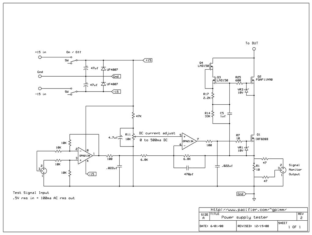
Schematic of the power supply tester:
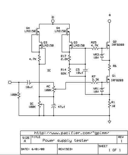 The DC pot is used to set the DC current loading the power supply or regulator under test. The AC pot allows the signal level to be set outside the sound card in the lab computer.
The Rev 1 power supply tester worked OK, but I wanted a power supply tester circuit that would interface better with the balanced sound card system in the lab computer and be capable of lower distortion operation.
By adding some circuitry using an OPA2134 opamp to interface with the balanced sound card and put the current control of the tester inside the feedback loop of the opamp the performance of the circuit was increased greatly. Using a resistor as a test load the harmonic distortion of the current output is less than .003%. Settings were 100ma draw and 33ma RMS AC current load with 100 volts across the power supply tester. The monitor output allows the test software to run in loop back mode using AC voltage across R1 as the reference voltage. This allows accurate measurements down to 1Hz and sets the 0dB level to 10 ohms.
The measurements below were made with the Rev1 power supply tester. Levels are relative. As time permits I will upload new measurements made with the Rev 2 power supply tester.
The first set of measurements is output impedance VS frequency. In this test the power supply tester was driven from the lab computer sound card. The Lab computer is equipped with an M-Audio Audiophile 192 sound card and a custom input signal processor box. The input signal processor box protects the sound card inputs as well as attenuate the incoming signal by 40dB, 20dB, 0dB, or amplify by 20dB. Audio Tester software is used for these measurements. Audio Tester was setup to sweep from 1Hz to 95Khz and use the right channel as a reference. Using the reference channel allows the sound card to measure very flat down to 1Hz.
The Swenson regulator circuit
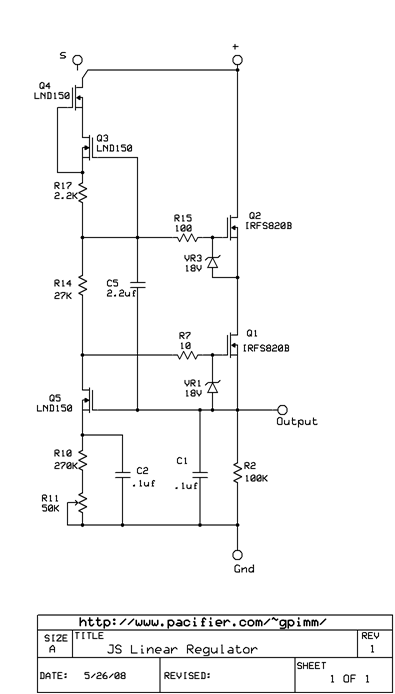
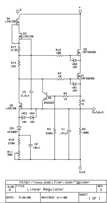
John created a very good voltage regulator based on the self bias CCS by slightly rearranging the bias string and adding an error amplifier to lower the output impedance. The error amplifier is the third LND150 (Q5). Q5 compares the output voltage of the regulator to the reference voltage on C2.
Changing the values of R10 and R11 sets the output voltage max and range. The circuit seems to be stable with 1ma minimum load.
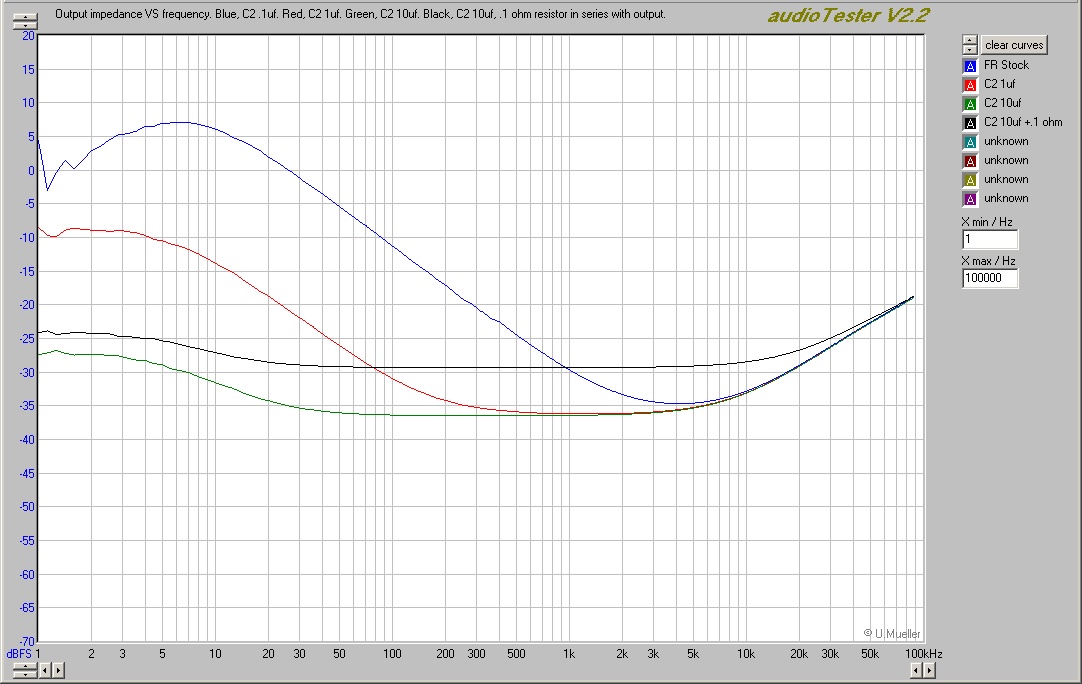
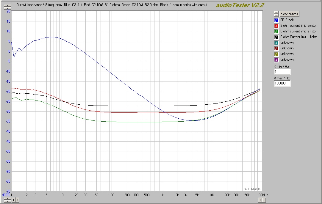
This screen shot shows the output impedance VS frequency for the regulator
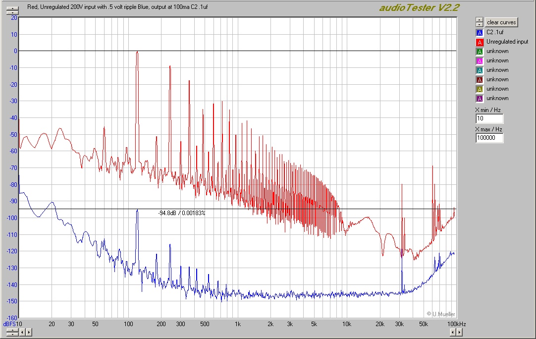
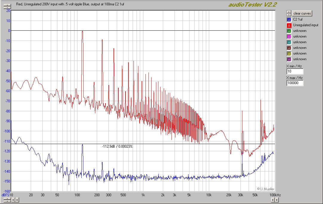
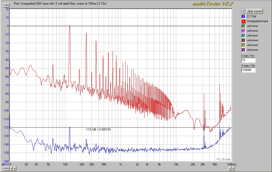
The basic test setup has the regulator powered from a 200V unregulated supply with .5 volt of ripple. The regulator is set for 100V output. The power supply tester is set to draw 100ma DC from the regulator. The AC signal is set to 34.6ma RMS (100ma P-P). This swings the load from 50ma to 150ma.
The blue trace is the response of the regulator with John's capacitor values. The red trace shows the response with C2 increased to 1uf. The green trace is with C2 increased to 10uf. The black trace is the same setup as the green trace except that a .1 ohm resistor was added to the output.
To measure the output impedance at 1Khz the power supply tester was set to draw 100ma DC and 20ma RMS AC. The AC ripple was measured with a o'scope then Ohm's law was used to calculate the impedance. With 20ma RMS signal applied the ripple on the regulator was 5.8mv p-p. Converting the P-P measurement on the scope to RMS> 5.8mv p-p/2*.707= 1.98mv RMS. Impedance = 1.98mv(E)/20mv(I)= .099 ohms.
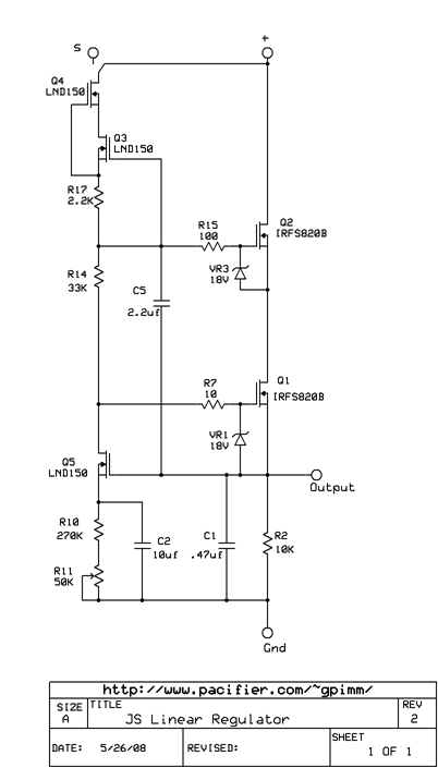
During the frequency sweeps there was some occasional instabilities. Increasing C1 to .47uf took care of the issue.
Updated schematic with the larger cap values
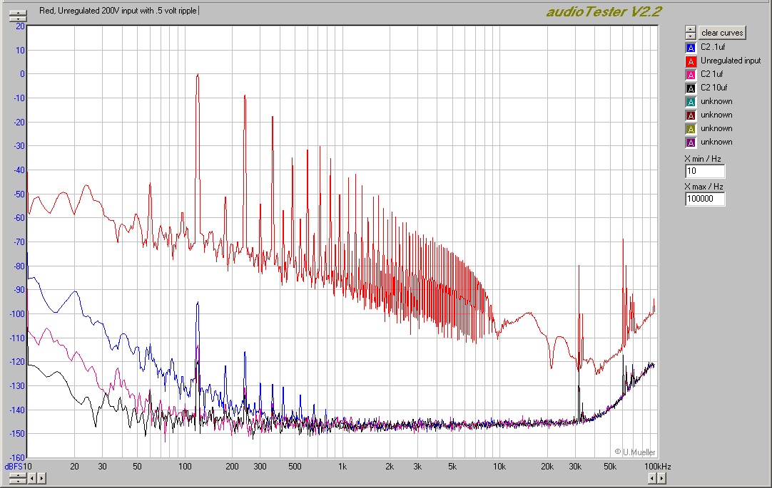
Ripple rejection. The next screen shot shows the regulators power supply rejection. Darn nice!
The setup for the ripple measurements has the input box set for 20dB of gain. The .5 volt of ripple was just over the sound card's input limit with the 20dB gain engaged so the unregulated input was captured with 0dB gain. The file from Audio Tester was massaged using Excel to add 20dB to the signal level. The main artifact from this manipulation shows up above 40Khz where the ripple met the sound card noise floor.
The power supply tester was drawing 100ma DC with no AC component for these tests.
The 3 traces overlaid are good to compare the 3 values of C2 but not good to try and see details.
Here are 3 screen shots each showing one value for C2 as well as the measurement of ripple rejection at 120Hz.
C2 .1uf
C2 1uf
C2 10uf
The regulator is performing very nicely but there is one issue left… If you short the output it blows up. I want to use several of these regulators to build a bench supply with multiple adjustable outputs. A bench supply has to be bullet proof!
The mostly bullet proof version…
First issue is gate protection for Q5. The 18V back to back zener diodes (VR3, VR4) provide protection for Q5. Another issue is the charge stored on C2. With a hundred or more volts on C2 there is a lot of energy stored. There is no way the protection zeners on Q5 would survive the surge of shorting the output. Adding a diode between Q5 and C2 removes the need to discharge C2 when the output gets shorted. If the output is shorted to ground D1 reverse biases and disconnects C2 from the circuit. R10 and R11 discharge C2.
The circuit also needs current limiting. Q6, R1, R3, and R4 are the current limit circuit. The output current causes a voltage drop across R1. When the voltage reaches around .5 volts Q6 starts to conduct removing gate drive from Q1 and shunting the reference bias current to the output causing the output voltage to drop.
To test the current limit the power supply tester was set to 100ma DC. The AC drive was increased until the output voltage dropped .1 volt. The current was measured with a DC current probe on the bench scope.
With R1 at 2 ohms the output current is hard limited to ~300ma. The first current limit circuit did not include R3, the fold back resistor. Without R3 in the circuit hard limit was 300ma but the current limit started working when the current peaks were at 170ma.
Adding R3 provides what is called fold back current limiting. When the output voltage is up a small current flows through R3 pulling the base of Q6 down about .24 volts. This allows the regulator to supply greater current when the voltage across the regulator is lower (i.e. normal operating). As the output voltage drops the current through R3 decreases allowing the current limit circuit to be more sensitive.
With the values shown in the schematic above the hard current limit is ~300ma but with the output at 100 volts the peak signal current can be as high as 420ma before the output voltage starts to drop.
To get the power supply tester to deliver the drive necessary for this test R1 had to be reduced to 5 ohms.
The only down side to the current limit circuit is the resistance of R1 reduces the tranconductance of Q1. This increases the output impedance some. The output impedance measurement with the current limit circuit in place shows the output impedance increased from .099 ohms to .142 ohms.
Frequency VS impedance with current limit circuit in place
You can see that the output impedance (Z) of the circuit with current limit (red trace) (.142 ohms output Z) fits between the green trace where the 2 ohm resistor is shorted out (.099 ohms output Z) and the black trace where a .1 ohm resistor is added (~.2 ohms output Z).
The regulator circuit with current limit is quite robust. I've repeatedly shorted the output to ground and it survives. Just keep in mind the power ratings of the output MOSFET. With 180 volts across Q2 and 300ma the power dissipation during the shorted condition in this test was 54 watts, way over the 33 watt limit. To set the hard current limit lower you can increase the value of R1.
In the development of the current limit and protection circuitry many, many parts let out their smoke before the regulator was close to «bullet proof».
Over all, this looks like a darn nice regulator. The output impedance is quite low without using large capacitors and the ripple rejection is suburb.
The high voltage version:
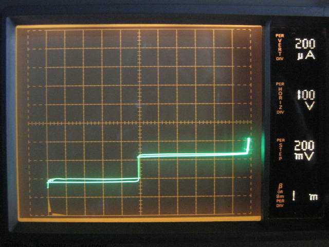
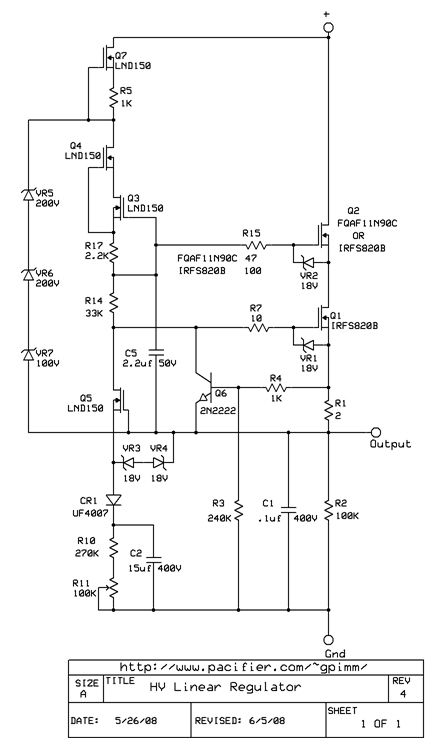
One of the things I wanted to use this regulator for is a new bench power supply. Wanting to have regulated outputs in the 500V+ range meant the input to the regulator was over the 500V limit of both Q2 and Q4. Replacing Q2 with any of the many 900V MOSFETs is easy. Coming up with a high voltage capable bias CCS was more interesting. The way I did this was to stack a third LND150 (Q7) on top of Q4 configured as a CCS set to deliver ~600ua. A string of zener diodes adding up to 500V is placed between the drain of Q4 and the output terminal of the regulator. When the input-output voltage is less than 500V the circuit works pretty much the same as the lower voltage version. The 3rd LND150 is «ON» and represents only a couple of K ohms in series with Q4. When the voltage goes over 500V the string of zeners turns on and clamps the voltage across the bias string to 500V above the regulator output voltage. Q7 now acts as a CCS and delivers ~600ua to the parallel combination of the Q4 bias string and the zener stack. This allows the input to Q7 to increase another 500V above the output voltage. In the test circuit Q4 was drawing 390ua with the remaining 210ua flowing through the zener stack.
Here is a screen shot from the Tek 576 curve tracer testing the high voltage bias regulator idea.
Below 500V the current drawn is the 390ua set by Q3. Above 500V the current increases to 620ua when Q7 becomes active. Just before 1100V you can see the current start to increase as Q7 starts to break down. During the whole sequence the current output from Q3 into the bias string remains constant.
Here is the schematic of the high voltage version.
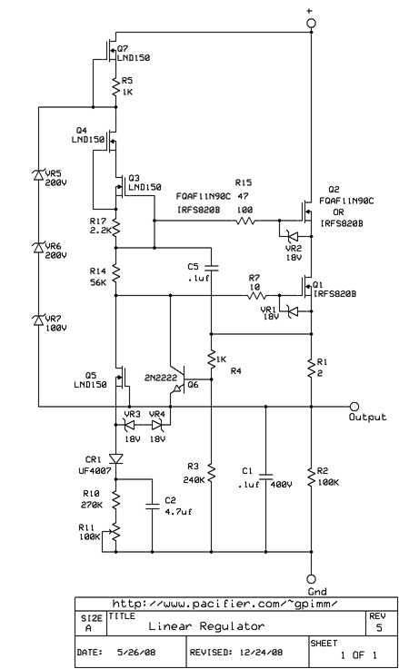
Over the winter break I was able to stuff and test 3 boards using the new board layout. During testing I found an error in the design that was limiting the performance some. When the 2 ohm current limit resister was added I wasn't paying close attention added the resistor between the Q1 MOSFET and C5, the cascode capacitor. In this configuration the error voltage across R1 was subtracted from the error amplifier Q5. By connecting the end of C5 back to the source of Q1 the performance increases. Also the increase of C1 to .47uf during early testing was found to not be necessary with the current limit resistor (R1) in circuit. C1 has been reduced back to .1uf. Another tweak was increasing R14 to 56K. This does 2 things- Increases the load on Q5 for higher gain for error correction and increases the voltage across Q1 improving the operating point of Q1. The third performance tweak was decreasing C5 to .1uf. This was counter intuitive at first but made sense after some thinking. The performance of the regulator starts roll off as the impedance of C2 increases at low frequencies. This can be seen in all the performance graphs above. The error amplifier Q5 is working into the load presented by R14 coupled to C5. This is 56K at higher frequencies. With C5 at .1uf the impedance of C5 starts to increase at ~50Hz. As the frequency decreases and the impedance of C5 increases the gain of Q5 increases at a rate that offsets the roll off caused by the rising impedance of C2. At the lowest frequencies Q5 is effectively CCS loaded by Q3 and Q4. With these changes and C2 at 4.7uf the impedance does not show the low frequency rise and is flat down to 1Hz , the limit I can measure to.
The circuit has been tested with an FQAF11N90 loaded in the Q2 location. This allows for higher voltage or power operation The only change is to lower R15 to 47 ohms.
The latest version of the regulator:
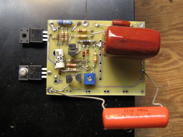
The board file, BOM, and a photo of the stuffed board is in a zip file and available for down load in the down load area.
To fit my desire to use of this regulator as a bench supply I've chosen film caps for C1 and C2. Reasons for using film caps are good high frequency performance and high voltage ratings are available. The caps chosen for this project are the Cornell Dubilier DME series miniature metallized polyester capacitors. They are relatively small for film caps. Values are available from Mouser up to 10uf at 250V and 2.2uf at 630V. Even though they are small for film caps they still take up a lot of real estate on the board. The board is setup so you can use multiple parallel caps for C2. C5, the electrolytic capacitor in the bias string is in a non critical location. It only needs to have a rating as it only sees the voltage across R14 + the turn on voltage of Q1.
Selectable resistor values:
R2 should be chosen to draw ~1ma at your chosen output voltage when using the IRF820B MOSFET in the Q2 location. If using the FQAF11N90 MOSFET the minimum current draw is 10ma. If you have lots of power available you can increase the current by using a shunt resistor on the output to ground. The output impedance of the regulator decreases as the current increases.
The bias current set by Q3 should be ~.35ma. The bias current will vary with each batch of LND150 MOSFETs. You can change the value of R1 to compensate for the variations in MOSFET lots. I've used the values from 2K to 2.4 K to get the bias current in the ball park.
R10 and R11 set the output voltage. The total resistance of R10 + R11 sets the output voltage. If you want only a small amount of adjustment make R10 be most of the resistance needed and R11 be a small portion. Just the opposite if you want a wide adjustment range. There are a couple of larger pads at R11 to facilitate connecting wires to an off board pot for panel mounting.
For high power or high voltage operation the board is setup to take either TO220 or T03P packages for Q2. I highly recommend the fully en capsulated parts for safety. The full encapsulation reduces the power disapation ratings but is made up by the ease of attaching to the heat sink without worry of arc-over and corona issues.
If you don't need to be able to handle over 500 volts on the input you can leave out Q7, R5, VR5, VR6, and VR7. Put a jumper wire across the drain and gate terminals of Q7 to connect the input voltage to Q4.
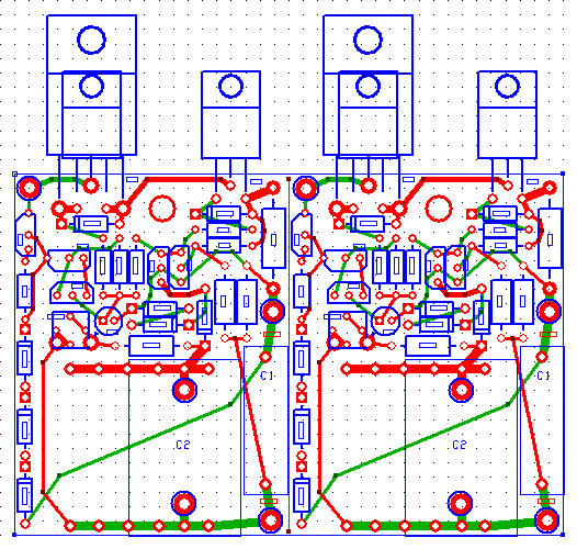
Here's the layout with 2 regulator boards an ExpressPCB mini board. After cutting the boards apart the board size is 2.5« high, 1.9»wide.
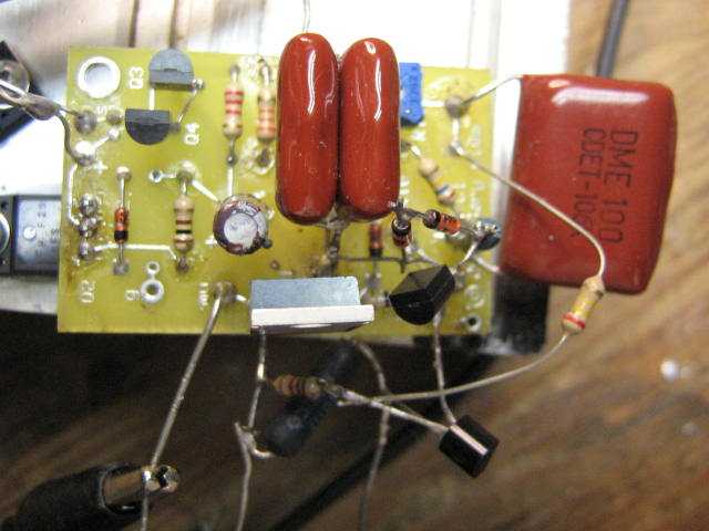
As is normal for regulators, you will need a local decoupling cap if the distance is more than a few inches from the filter cap. In my bench testing where several 12« clip leads were used between the bench supply and the regulator being tested it was necessary to have a .1uf capacitor across the regulator as seen in the photo below.
Photo of the board stuffed showing how to connect C5 for the updated schematic.
Ugly abused test mule…
Усилитель на 300B
In Rev 3 the I added a shunt regulator driven by a CCS on the driver stage. This rates as one of the biggest improvements so far. The dynamics are really wild now. The background is blacker than ever and I'm hearing things I've never heard before. Bass has taken on a whole new personality, it feels totally bottomless. Kick drums are great. This is a SET that never looses it's composure no mater how crazy things get.
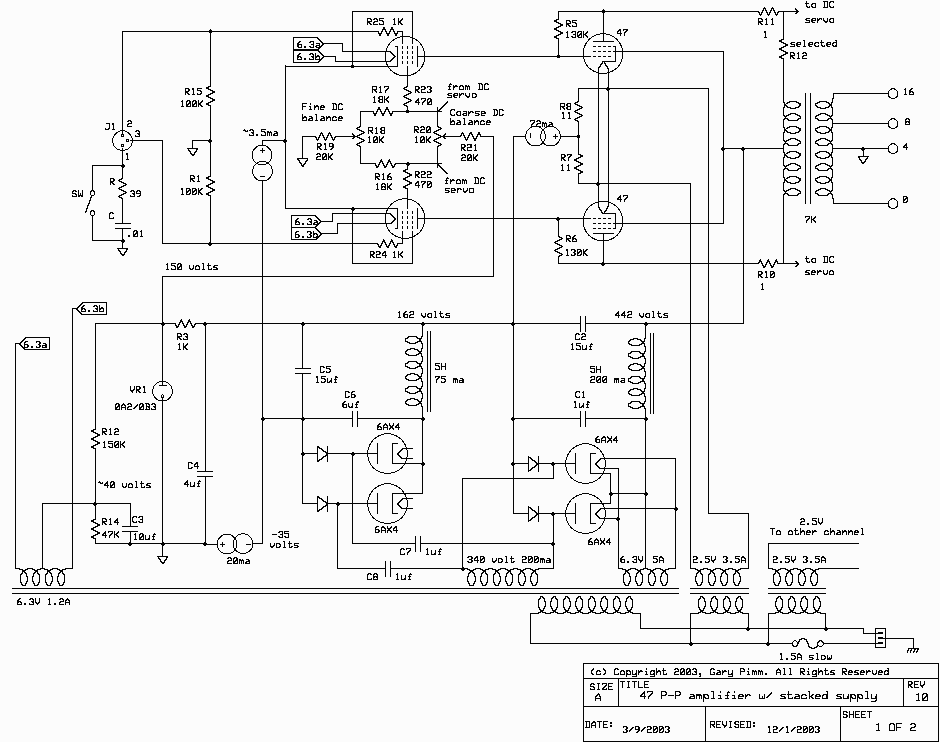
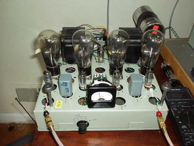
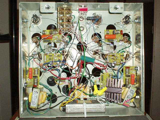
Усилитель на 47 пентодах
The new power supply is performing very well. The power transformer and the output CCS's are running cooler and the input pentodes are at a much better operating point. All the concerns about the old power supply have been addressed.
The only thing that needs to be addressed it turn on hum. The plate to cathode voltage of the output tubes is set by the current flowing through the feedback resistors. This current is determined by the CCS on the input tubes. The input stage is at full operating current rather quickly and this forces the output stage to try to set the plate to cathode voltage to the standard operating point before the voltage is available. This starves the output CCS of voltage. When the current is below the set level on a battery biased CCS the CCS looks like a resistor with the value of (R1+5 ohms), or in this case about 130 ohms. Everything gets quiet as soon as there is voltage for the output CCS.
The fix for this (I think) is going to be to use the mosfet only version of the Rev 5 CCS on the input stage. It starts in the off state and slowly increases the current up to the operating point, which is the opposite of the battery biased CCS. The battery biased CCS is on hard until the current increases above the set point. By increasing the value of C5 in the Rev 5 CCS the turnon time increased. The right size cap should delay the input stage reaching full operating current and stop the hum during startup. The only thing that is keeping me from trying this out is I have run out of space inside the prototype case. The darn thing is full!
Sound wise, it sounds just a touch cleaner and more dynamic.
**
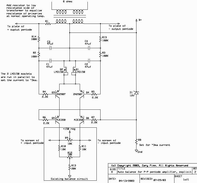
Here is the autobalance servo circuit. Basically, it senses the current in the output tubes by the DC voltage drop across the primary of the transformer. Because it is using the primary for the sense, if the resistance of the 2 halves of the primary don't match you need to add resistance to the low side to make it match with the high side. This must be done with the transformer warmed up to normal operating temp.
When the circuit is balanced the differential amplifier (Q3,Q4) sends equal amounts of the ~3ma bias current provided by the LND150's through both transistors. If the amplifier drifts off center the differential amp will increase the current delivered to the screen of the side of the amp that is drawing more current. This turns the input pentode on harder on that side which in turn pulls down on the grid of the output tube on that side, decreasing the current it draws.
The auto-balance circuit connects to the screens of the input pentodes and works with the DC balance pots. Once you adjust the output balance it does not drift more than .5ma after warm-up.
Q5 and Q6 provide both level shifting and cascode isolation to the differential amp (Q3, Q4) The transistors used for Q3 and Q4 are now BC560's. They have a much higher gain than the 2N2907's.
Усилитель на 6BQ5
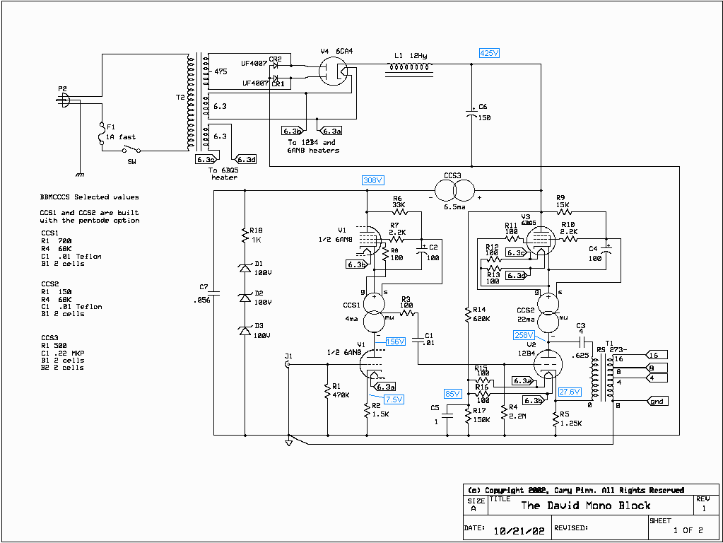
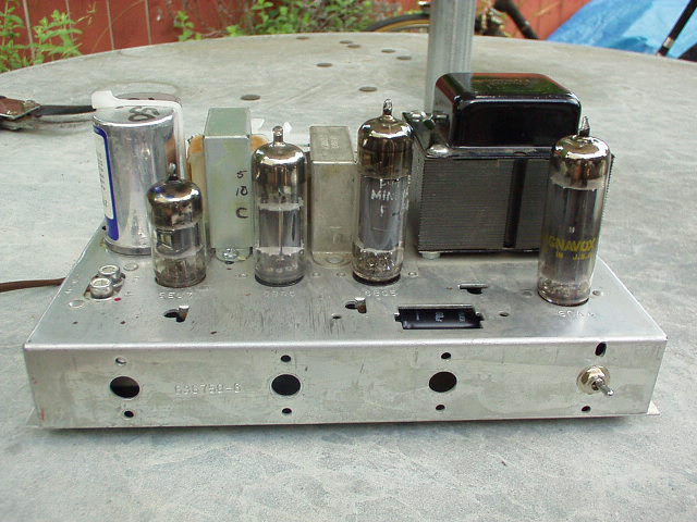
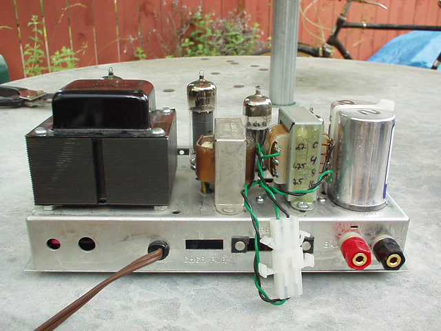
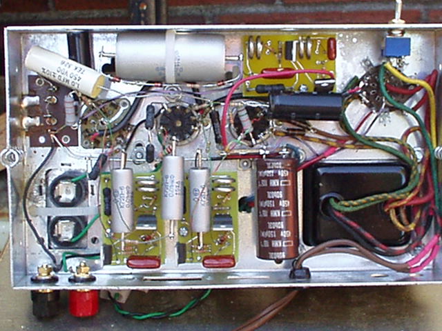
The David project was an entertaining exercise in how much stuff can be crammed into a small box… The donor chassis' were a pair of Motorola SE 6BQ5 stereo amps. One of the amps came from a Motorola mini console, the other amp came from an AMC mini console.
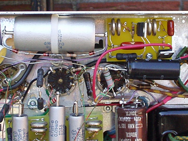
In each amp the power supply was changed to a full wave bridge with choke input to get the supply voltage up for the active loading. One of the 6BQ5's was retained as the output stage CCS. One of the original SE output transformers was used as the power supply choke. Managed to cram 3 CCS boards into the chassis… The output transformer is a 70 volt line matching transformer, the cheap one that Radio Shack used to sell.
The David uses a 6AN8 triode/pentode as the input tube. The triode section is used as the input stage while the pentode section is used as the CCS for the input stage. The input stage is RC coupled to the EL84 CCS loaded 12B4 triode output stage. The driver stage of the David has a CCS fed shunt regulated power supply.
The pair of David monoblocks are used as my lab amps and see almost daily use. They put out 1 clean watt that is very transparent and has great bass. At full power of 1 watt the frequency response is 30 to 22K, at low power levels the response is better going from ~20 to 30K.
One of my friends uses a pair of David's to power his Klipsh LaScala's. More power than he needs in a small room ;-}
The schematic…
"Каменный" вариант
http://www.pimmlabs.com/web/solid_state.htm
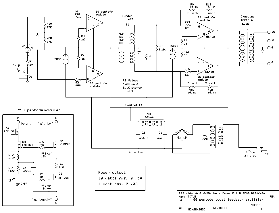
Quite awhile back I got an email from John Swenson asking if the active circuitry used in the self bias could be used as an amplifier. I mentioned that I thought it would work and in fact had thought of the ideas several times in the past but had never pursued the idea. John went on to do experiments and came up with several interesting tranconductance amplifier ideas.
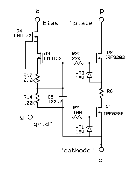
After hearing of his successes I decided to try some ideas of my own. One of the early experiments was to compare a single IRF820b MOSFET to a modified self bias CCS amplifier. I started calling the basic building block the Solid State Pentode based on the way the circuit works.
While the characteristic curves of single MOSFETs looks very Pentode like they do not have the low input capacitance of a Pentode. The cascode circuit below acts very much like an ideal Pentode as the gate to source capacitance of the upper MOSFET is shunted to the source of the lower MOSFET via C5.
Here is the schematic of the basic SSP building block.
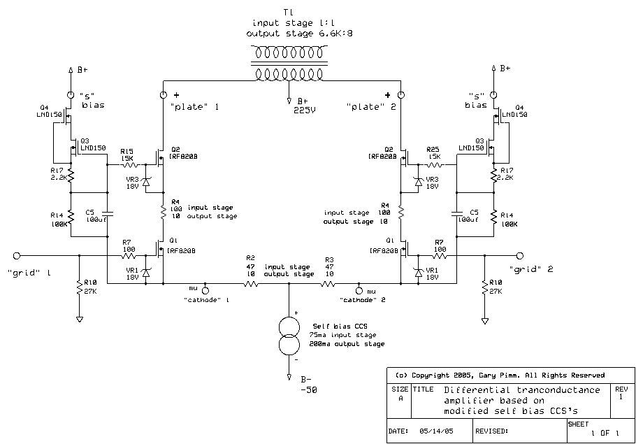
The next experiment was a CCS loaded differential stage. This stage is a tranconductance amplifier, meaning that an input voltage is converted to an output current. The goal was building a solid state version of the Tabor amplifier with an interstage transformer between the input and output stage. I was using 6.6K as the load for the input stage as this is what the estimated input impedance of the Tabor output stage. Later I substituted a 6.6K output transformer and found that by increasing the operating current and B+ voltage the single stage could deliver 10W into 8 ohms at quite low distortion. Not bad for a single stage amplifier. The output impedance is very high. With the amplifier delivering 10V rms into 8 ohms I clipped a second 8 ohm load resistor in parallel dropping the load impedance to 4 ohms. The output voltage dropped to 5V rms.
Here is the schematic of the input tranconductance stage with values for both input stage and tranconductance output stage amplifier uses.
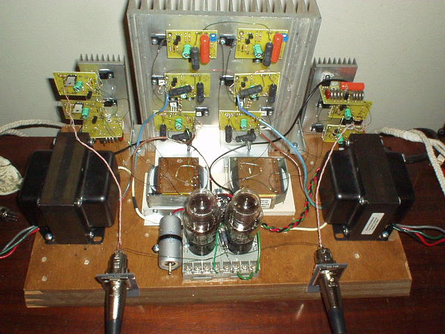
After the success of the input stage I wanted to mate it to the output stage and see the results. Here is the schematic of the first prototype of the «Solid State Tabor».
